| CMOS Design > I/O Interface Design |
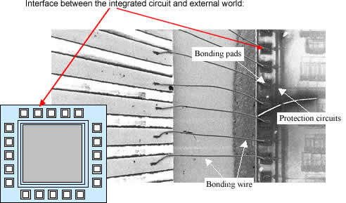
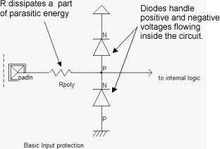
We give here some details about input-output pad structure. The basic bonding pad size is 100x100µm. The pad consists of a sandwich of metal layers. For advanced technologies, all metal layers are stacked on the top of each other. The passivation oxide has been removed from over the pad, so that a gold connection can be fixed upon it. The input-output pad contains one input stage with a polysilicon resistor and two protection diodes. The output stage contains a chain of inverters. The last stage is a 3-state inverter so that the buffer can be turned off.
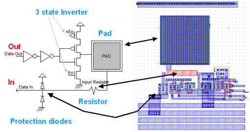
The resistor made in diffusion has a value between 10Ω and 500Ω. Its role is to limit the current.
The diodes are used to limit the input voltage between Vdd + Vt and Vss - Vt and to protect from electro static discharge (ESD) which may be as high as 5000V!
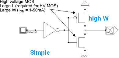
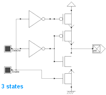
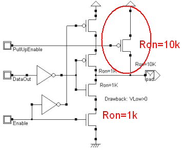
An example of output pad is shown in this figure. It only consists of a n-channel MOS and a p-channel MOS device with large width to drive large currents. The 3-state function is provided by two extrat MOS devices, one p-MOS on the VDD path, one n-MOS on the ground path. When both pass transistors are on (Enable=1), the pad works as a normal output pad. When enable=0, the pad is isolated from both VDD and VSS.
| Goal : To ensure that the signal is propagate out of the chip safely |
|
The current drive of the output pad is an important parameters for low-power application. Using a 2mA current limits the power dissipation but provokes low speed switching. When 2mA and 4mA drivers work simultaneously, a 6mA current is available to charge and discharge the output signal faster, at the cost of a higher power dissipation.
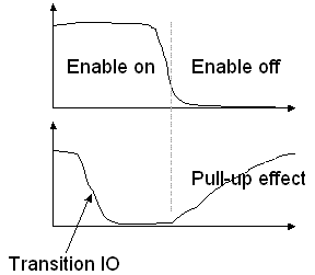
It is usual to add a pullup device, to ensure a weak link to VDD, mainly in the case of 3-state configuration. The pull-up ties the output to VDD through a 10KΩ equivalent resistance at least 1a times larger than the normal output MOS Ron resistance.
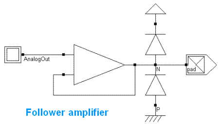
There exist also specific pads for analog output. A susal analog pad includes a wide range amplifier connected as a voltage follower. Diodes are added to limit the under and over voltage stress.
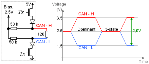
An application-oriented i/o structure is presented here. The Control Area Network (CAN) I/O is widely used in automative. Several specific features are included: a two-state differential output, one which ties CAN-L to 1.5V, and CAN-H to 3.5V, the other state which disables the power MOS and links the bus to a weakly tied 2.5V, almost equivalent to a high impedance state.
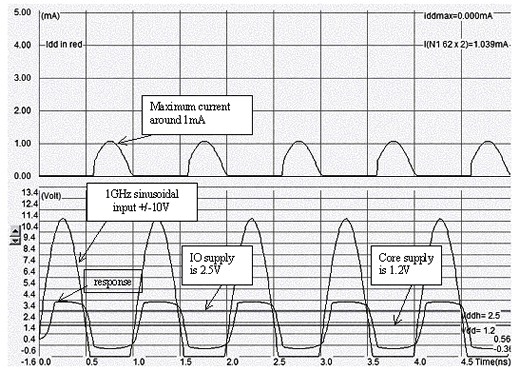
The input circuit of an IC always use thiht voltage logic gates, which use thick oxide to enhance the handling of over voltage. To limit the electrostatic discharge stress, Zener Diodes and shunt resistors are commonly used.
The effect of the Zener Diode is to limit both the overvoltage (Zener in reverse mode) and the undervoltage as shown in the simulation.
| CMOS Design > I/O Interface Design > I/O Interface |