EEPROM Memory
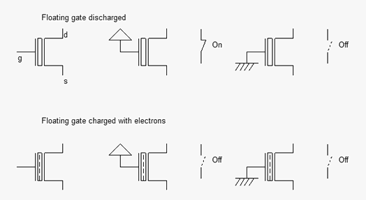
The basic element of an EEPROM (Electrically Erasable PROM) memory is the floating-gate transistor. The concept was introduced several years ago for the EPROM (Erasable PROM). It is based on the possibility of trapping electrons in an isolated polysilicon layer placed between the channel and the controlled gate. The charges have a direct impact on the threshold voltage of a double-gate device. When there is no charge in the floating gate (Figure 10-74, upper part), the threshold voltage is low, meaning that a significant current may flow between the source and the drain, if a high voltage is applied on the gate. However, the channel is small as compared to a regular MOS, and the Ion current is 3 to 5 times lower, for the same channel size.
 |
| Figure 10-74: The two states of the double gate MOS |
When charges are trapped in the floating polysilicon layer (Figure 10-74, lower part), the threshold voltage is high, almost no current flows through the device, independently of the gate value. Data retention is a key feature of EEPROM, as it must be guaranteed for a wide range of temperatures and operating conditions. Optimum electrical properties of the ultra thin gate oxide and inter-gate oxide are critical for data retention. The typical data retention of an EEPROM is 10 years.
 |
 |
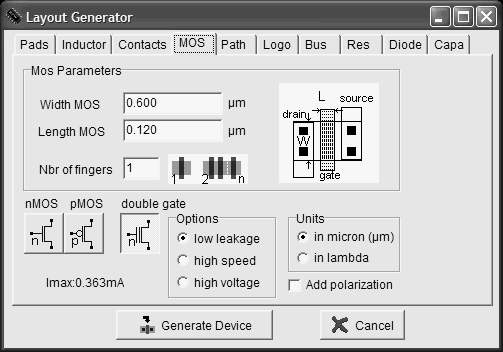
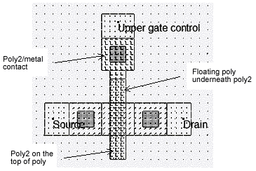
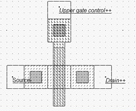
| Figure 10-75: The double gate MOS generated by Microwind |
 |
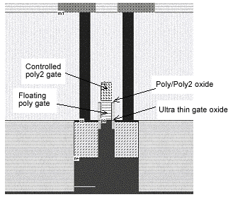
| Figure 10-76: Cross-section of the double gate MOS |
The double gate MOS layout is shown in figure 10-75. The structure is very similar to the n-channel MOS device, except for the supplementary poly2 layer on the top of the polysilicon. The lower polysilicon is unconnected, resulting in a floating node. Only the poly2 upper gate is connected to a metal layer through a poly2/metal contact, situated on the top. The cross-section of figure 10-77 reveals the stacked poly/poly2 structure, with a thin oxide in between.
The programming of a double-poly transistor involves the transfer of electrons from the source to the floating gate through the thin oxide (Figure 10-78). Notice the high drain voltage (3V) which is necessary to transfer to some electrons enough temperature to become "hot" electrons, and the very high gate control to attract some of these hot electrons to the floating poly through the ultra thin gate oxide. The very high voltage varies from 7V to 12V, depending on the technology. Notice the "++" symbols attached to the upper gate and drain regions, which indicate that a voltage higher than the nominal supply are used.
 |
 |
| Figure 10-78: The floating gate is charged with hot electrons thanks to a tunneling effect through the ultra-thin gate oxide |
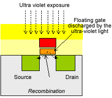
The floating gate may be discharged by ultra violet light exposure or by electrical erasure. The U.V. technique is an heritage of the EPROM, which requires a specific package with a window to expose the memory bank to the specific light. The process is very slow (Around 20mn). After the U.V exposure, the threshold voltage of the double gate MOS returns to its low value which enables again the current to flow (Figure 10-80).
 |
 |
| Figure 10-80: The floating gate may be discharged by U.V light exposure |
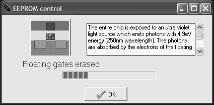
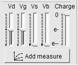
In Microwind, the command Simulate > U.V exposure to discharge floating gates simulates the exposure of all double gate MOS to an ultra violet light source. At the end of the simulation (Which takes 10 seconds instead of 20 minutes in reality!), all floating gates of the layout are discharged. Alternatively, the charge contained in the floating gate can be accessed individually using the command Simulate > Mos characteristics. On the right lower corner of the device characteristics, a cursor named Charge appears, representing the amount of electrons stored in the floating gate. Changing the cursor position (Which corresponds in figure 10-81 to the minimum charge of electrons) modifies dynamically the MOS characteristics.
 |
| Figure 10-81: Access to the double gate electron charge |
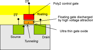
For the electrical erase operation, the poly2 gate is grounded and a high voltage (Around 8V) is applied to the source. Electrons are pulled off the floating gate thanks to the high electrical field between the source and the floating gate. This charge transfer is called Fowler-Nordheim electron tunneling (Figure 10-82).
 |
| Figure 10-82: Discharging the double gate MOS device |
