Programmable Logic Block
The programmable logic block consists of a look-up table, a D-register and some multiplexor. There exist numerous possible structures for logic blocks. We present in figure 9-15 a simple structure, which has some similarities with the Xilinx XC5200 series (See [Smith] for detailed information on its internal structure). The configurable block contains two active structures, the Lut and the D-reg, that may work independently or be mixed together.
The output of the look-up-table is directly connected to the block output Fout. The output can also serve as the input data for the D-register, thanks to the multiplexor controlled by DataIn_Fout. The DataOut net can simply pass the signal DataIn, in that case the cell is transparent. The DataOut signal can also pass the signal nQ, depending on the multiplexor status controlled by DataIn_nQ.
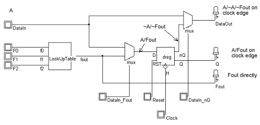 |
| Figure 9-15: Simple configurable logic block including the Look Up Table and a D-register |
The block now consists of the LUT and the D-register. We chain the information DataIn_Fout and DataIn_nQ on the path of the shift register by adding 2 supplementary Dreg cells. Each Dreg still uses the same clock ClockProg and chained input data DataProg. The complete circuit is shown in figure 9-16.
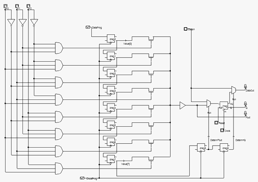 |
| Figure 9-16: The Look Up Tablem the D-register and the shift register including the 2 multiplexor cells |
The configuring of the block is realized thanks to 10 active clock edges on ClockProg, and 10 serial data on DataProg. The chain of Dreg starts at Dreg0 (Upper Dreg in figure 9-16, which produced Value[0]) and stops at Dreg9 (Right side of figure 9-16, which produced DataIn/nQ). The information that flows at the far end of the register chain is defined at the first cycle, while the closest register is configured by the data present at the last active clock edge.
 |
| Clock cycle |
1 |
2 |
3 |
4 |
5 |
6 |
7 |
8 |
9 |
10 |
| DataProg |
DataIn/Nq |
Datain/Fout |
Val[7] |
Val[6] |
Val[5] |
Val[4] |
Val[3] |
Val[2] |
Val[1] |
Val[0] |
|
| Table 9-3: Serial data information used to program the LUT memory points |