Configurable Logic Circuits
The programmable logic block must be able to implement all basic logic functions, that is INV, AND, NAND, OR, NOR, XOR, XNOR, etc... Several approaches are used in FPGA industry to achieve this goal. The first approach consists in the use of multiplexor, the second one of look-up tables.
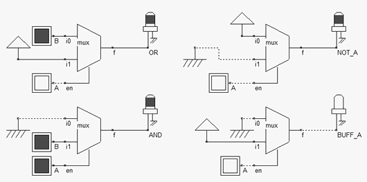
Surprisingly, a two-input multiplexor can be used as a programmable function generator, as illustrated in table 9-1. Recall that the multiplexor output ƒ is equal to i0 if en=0, and i1 if en=1. For example, the inverter is created if the multiplexor input i0 is equal to 1, i1 is equal to 0, and enable is connected to A. In that case, the output ƒ is the ~A. The figure 9-5 describes the use of multiplexor to produce the OR, AND, NOT and BUF functions.
| Function |
Boolean expression for output f |
i0 |
i1 |
en |
| BUF(A) |
f=A |
0 |
A |
1 |
| NOT(A) |
f=~(A) |
1 |
0 |
A |
| AND(A, B) |
f=A&B |
0 |
B |
A |
| OR(A, B) |
f=A | B |
B |
1 |
A |
|
| Table 9-1: Use of multiplexor to build logic functions |
 |
| Figure 9-5: Use of multiplexor to build logic functions |
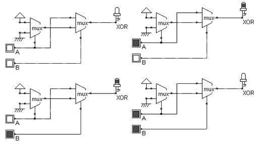
Although NOT, AND and OR are directly available, other functions such as NAND, NOR and XOR cannot be built directly using a single 2-input multiplexor, but need at least two multiplexor circuits.
 |
| Figure 9-6: The XOR gate build from 2 multiplexor circuits |
The XOR function is shown in figure 9-6. The 4-input XOR gate would require 6 multiplexor cells. Remember that each multiplexor cell consists of a minimum of 6 transistors for a buffered output, and has 3 delay stages (The two inverters and the pass transistor). The XOR4 implementation would comprise a total of 18 delay stages, which is far too important. Therefore, the multiplexor approach is not very efficient for many logical functions.
The look-up table (LUT) is by far the most versatile circuit to create a configurable logic function. The look-up table shown in table 9-2 has 3 main inputs F0,F1 and F2. The main output is Fout, which is a logical function of F0, F1 and F2. The output Fout is defined by the values given to Value[0]..Value[7]. The three values F0,F1, F2 create a 3-bit address i between 0 and 7, so that Fout gets the value of Value[i]. In the example of table 9-2, the input creates the number 5, so Value[5] is routed to Fout. The table below gives Value[i] for the most common logical functions of F0,F1 and F2.

| Function |
Value [0] |
Value [1] |
Value [2] |
Value [3] |
Value [4] |
Value [5] |
Value [6] |
Value [7] |
| ~F0 |
0 |
1 |
0 |
1 |
0 |
1 |
0 |
1 |
| ~F1 |
0 |
0 |
1 |
1 |
0 |
0 |
1 |
1 |
| ~F2 |
0 |
0 |
0 |
0 |
1 |
1 |
1 |
1 |
| F0&F1 |
0 |
0 |
0 |
1 |
0 |
0 |
0 |
1 |
| F0 | F1 | F2 |
0 |
1 |
1 |
1 |
1 |
1 |
1 |
1 |
| F0^F1^F2 |
0 |
1 |
1 |
0 |
1 |
0 |
0 |
1 |
|
| Table 9-2: Link between basic logic functions and |
In the case of the 3-input XOR, the set of values of Fout given in the truth-table of table 9-3, must be assigned to Value[0]..Value[7]. In the schematic diagram shown in figure 9-7, we must assign manually the Fout truth-table to each of the 8 buttons. Then Fout produces the XOR function of inputs F0, F1 and F2.
| F2 |
F1 |
F0 |
Fout=F0^F1^F2 |
Assigned to |
0 |
0 |
0 |
0 |
Value [0] |
0 |
0 |
1 |
1 |
Value [1] |
0 |
1 |
0 |
1 |
Value [2] |
0 |
1 |
1 |
0 |
Value [3] |
1 |
0 |
0 |
1 |
Value [4] |
1 |
0 |
1 |
0 |
Value [5] |
1 |
1 |
0 |
0 |
Value [6] |
1 |
1 |
1 |
1 |
Value [7] |
|
| Table 9-3: Truth-table of the 3-input XOR gate for its implementation in a look-up-table |
 |
| Figure 9-7: The output f produces a loical function Fout according to a look-up-table stored in memory points Value[i] |
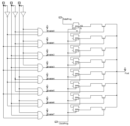
Memory points are essential components of the configurable logic blocks. The memory point is used to store one logical value, corresponding to the logic truth table. For a 3-input function (F0,F1,F2 in the previous LUT), we need an array of 8 memory points to store the information Value[0]..Value[7]. There exist here also several approaches to store one single bit of information. The one that is illustrated in figure 9-8 consists of D-reg cells. Each register stores one logical information Value[i]. The Dreg cells are chained in order to limit the control signals to one clock ClockProg and one data signal DataProg. The 8 logical information Value[i] are fully programmed by a word of 8 bits sent in series to the signal DataProg.
 |
| Figure 9-8: The look-up information is given by a shift register based on D-reg cells |
The configuration of the 3-input LUT into a 3-input XOR gate obeys to a strict protocol described in figure 9-9. A series of 8 active edges is generated by the ClockProg signal (Dreg is active on fall edges). This is done by configuring a pulse generator with series of 0-1 as shown below.
 |
| Figure 9-9: Programming the ClockProg pulse to generate 8 active edges |
At each active edge, the shift register is fed by a new value presented sequentially at input DataProg. As the D-reg is active on fall edge, data may be changed on each rise edge. Notice that the last Dreg corresponds to Value[7]. Therefore, Value[7] must be inserted first, and Value[0] last. This means that the DataProg pulse must describe the truth table in reverse order, as shown below.
 |
| Figure 9-10: At the end of the 8-th clock periodm the LUT is configured as a 3-input XOR |
In DSCH, a look-up-table symbol is proposed in the symbol menu (Figure 9-14). It is equivalent to the schematic diagram of figure 9-8. An important property of the LUT symbol is its ability to retain the internal programming as a non-volatile memory would do. The user's interface of the LUT symbol is given in figure 9-14. There are three ways to fill the look-up-table: one consists in defining each array element with a 0 or a 1. The number corresponds to the logic combination of inputs F2,F1,F0. For example the n°4 is coded 100 in binary, corresponding to F2=1,F1=0 and F0=0. A second solution consists in choosing the function description in the list. The logic information Fout assigned to each combination of the inputs updates the look-up-table. A third solution is also proposed: the user enters a description based on inputs F0,F1 and F2, and the logic operators "~" (Not), "&' (And), "|" (Or) and "^" (Xor). Then, click the button "Fill LUT" to transfer the result of the expression to the table.
 |
 |
| Figure 9-14: The look-up-table symbol |