The World of Memories
Semiconductor memories are vital components in modern integrated circuits. Stand-alone memories represent roughly 30% of the global integrated circuit market. Within system-on-chip, memory circuits usually represent more than 75% of the total number of transistors.
 |
| Figure 10-1: Major classes of CMOS compatible memories |
Two main families of devices exist: volatile and non-volatile memories. In volatile circuits (Figure 10-1 left), the data is stored as long as the power is applied. The dynamic random access memory (DRAM) is the most common memory. When the power supply is turned off, the information is lost. Non-volatile memories are capable of storing the information even if the power is turned off (Figure 10-1 right). The read-only memory (ROM) is the simplest type of non-volatile memory. One-time programmable memories (PROM) are a second important family, but the most popular non volatile memories are erasable and rogrammable devices: the old electrically programmable ROM (EPROM), the more recent Electrically Erasable PROM (EEPROM, FLASH), and the new magneto resistive RAM (MRAM) and ferroelectric RAM (FRAM) memories
Millions of elementary memories are used by microprocessors for executing of software. Micro-code, operating systems and low level software are usually stored in non-volatile memory. The software execution requires fast-access random access memory such as static or dynamic RAM. Memory exist as stand-alone components (Figure 10-2-a), but also as embedded blocks in system-on-chip, such as shown in figure 10-2-b.
 |
| Figure 10-2: The memory exists as a stand-alone component and an embedded block |
Memory organization
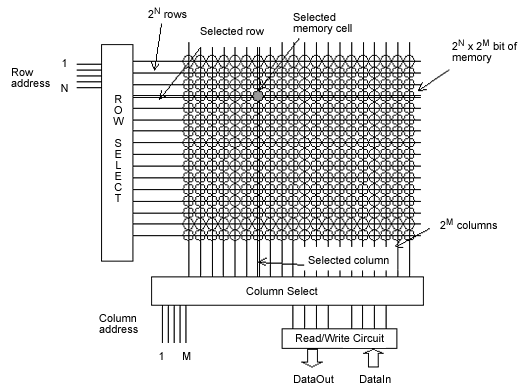 |
| Figure 10-3: Typical memory organization |
Figure 10-3 shows a typical memory organization schematic. It consists of a memory array, a row decoder, a column decoder and a read/write circuit. The row decoder selects one row from 2N, thanks to a N-bit row selection address. The column decoder selects one row from 2M, thanks to a M-bit column selection address. The memory array is based on 2N rows and 2M columns of a repeated pattern, the basic memory cell. A typical value for N and M is 10, leading to 1024 rows and 1024 columns, that corresponds to 1048576 elementary memory cells (1Mega-bit). Several organization exist: 1024x1024 bit, 128Kx8bit, 64Kx16bit, 32Kx32 bits, etc.. For example, the organization 128Kx8bit consists in selecting 8 columns in parallel. In that case, the size of DataOut and DataIn bus is 8 bit.
Access Time
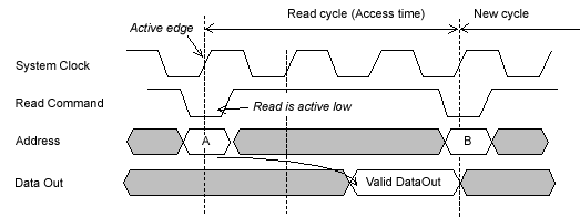 |
| Figure 10-4: Read Access Time |
The typical timing diagram of a memory block is shown in figure 10-4. A fast system clock, around 1GHz period, synchronizes the whole sequence. On an active level of the Read command (Usually a low level), the read cycle begins. It may take several clock cycles before the data is available. In the case of figure 10-4, two clock cycles are necessary before the valid data is proposed at the DataOut bus. The typical access time for Mega-bit memories ranges between 1ns and 10ns.