| Radio-Frequency Circuits > Frequency Converter |
In many situations for radio frequency emitters and receivers, there is a need for shifting a input waveform into a lower or higher frequency waveform. From an emission point of view, most of the signal processing is done within the range 10-100MHz. However, the emission bandwidth may be significantly higher (900MHz, 1.8GHz for mobile, 2.4, 5GHz for wireless local area network). A direct generation of the desired signal at such a high frequency would consume too much power. A low power frequency translator circuit is preferred. In the case of figure 12-67, the frequency converter shifts the original signal (Say 100MHz) to the desired emission frequency 900MHz.
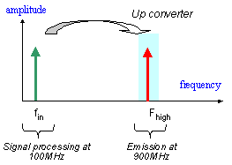 |
| Figure 12-67. The principles for frequency conversion |
The operation which translates a high frequency signal into a low frequency signal is called down conversion. In frequency domain, it consists in shifting a high frequency information contained in frequency fin to a lower frequency flow, as illustrated in figure 12-68. The information contained in the original signal fin (Which may include an amplitude, frequency or phase variation) is preserved in the resulting signal fout.
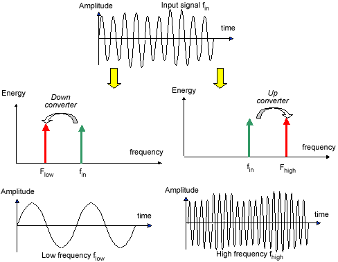 |
| Figure 12-68. The principles for frequency conversion |
Adding sinusoidal waves is very easy. A simple circuit containing 3 resistor produces the addition of two sinusoidal waves, as shown in figure 12-12. The formulation is easily demonstrated using the superposition theorem.
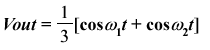 |
(Equ. 12-12) |
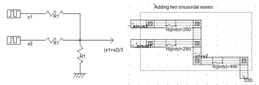 |
| Figure 12-69.Adding sinusoidal waves is easy, a set of 3 resistors is sufficient to build the sum |
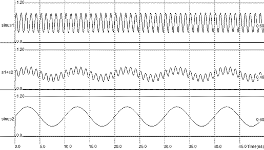 |
| Figure 12-70. The simulation of the sinusoidal wave adder |
The Fourier transform of the signal s1+s2 reveals two harmonics (Figure 12-71), one at the frequency of signal 1, the other at the frequency of signal 2, as the formulation 12-12 suggested. Clearly, no frequency shift may be obtained using sinusoidal addition.
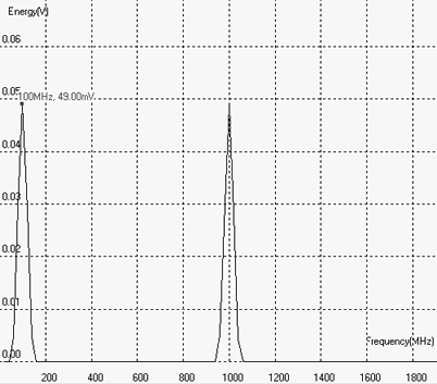 |
| Figure 12-71. The Fourier transform of s1+s2 reveals two harmonics, one at 100MHz the other at 1GHz |
At the core of up/down frequency conversion is the multiplication of two sinusoidal waves in the time domain [Lee Chapter 12]. The result of that multiplication is the generation of two new frequencies: one at the sum of frequency, one for the difference.
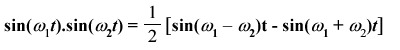 |
(Equ. 12-13) |
| where ω1=2π.f1 ω2=2π.f2 f1 = frequency of signal 1 (Hz) f2 = frequency of signal 2 (Hz) | |
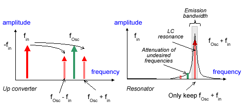
If we consider a low frequency fin, and a high frequency fOsc and only consider absolute values, the multiplication of these two sinusoidal signals creates two new sinusoidal contributions: one at fOsc -fin, one at fOsc + fin (Figure 12-72). Using an LC resonant circuit, we only keep the desired frequency contribution. In the case of figure 12-72, the L and C values are tuned to highlight the fOsc + fin contribution, which fits with the emission bandwidth. The LC resonator also serves as a filter of undesired harmonics, such as fOsc - fin and fOsc.
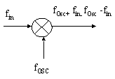  |
| Figure 12-72. The multiplication of two frequencies create new frequency components |
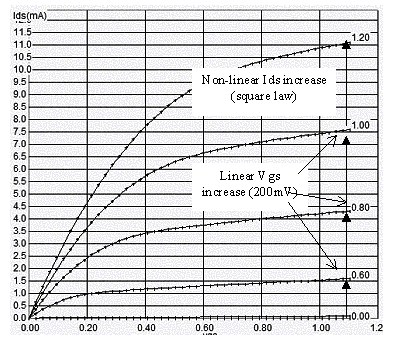
The process for multiplying signals with CMOS devices is far from being simple. The nMOS and pMOS are non-linear devices. The best example is the long channel nMOS which gives approximately a square law dependence between Vgs-Vt and Ids, as illustrated in figure 12-73. A linear device would give a linear dependence between Ids and Vgs, which is almost the case for short-channel devices. See chapter 3 for more details about device modeling.
 |
| Figure 12-73. The long-channel MOS characteristics exhibit a square dependence of Ids vs. Vgs |
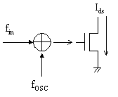
The idea is as follows (Figure 12-74): the two sinusoidal inputs fin and fOsc are added on the gate Vgs. The current Ids is a non linear function of Vgs. The static characteristics of the device (W=50µm, L=0.5µm) show a "quadratic" dependence: each Vgs step induces a square increase of Ids. This can be simply written as:
| (Equ. 12-14) | |
| where k depends on the design and technology Vt is the threshold voltage (Around 0.35V) |
|
 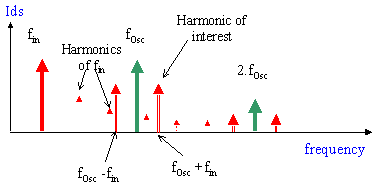 |
| Figure 12-74. The Ids current exhibits several harmonics, including the desired high frequency fOsc+fin |
If Vgs is a sum of sinusoidal waveforms, as we did in the previous section, the current may be written as:
| (Equ. 12-15) | |
| (Equ. 12-16) | |
 |
(Equ. 12-17) |
The most important result beyond this approximation is that the input signal and the oscillator signal are effectively multiplied and create the desired harmonics. In other words, passing a sum of sinusoidal waveforms into a non-linear device create several harmonics, from which fin+fOsc and fin-fOsc are the most important. The desired harmonic is underlined in equation 12-17 by rearranging the product of sinus into a sum of sinus. The term Ids0 also contains the original input signal, the oscillator signal and all their respective harmonics too, which lead to a quite complex output. A band-pass filter is mandatory to eliminate undesired harmonics and amplify the desired signal. The circuit is called a single-balanced mixer.
The n-channel MOS implemented in the mixer layout must have a large length to eliminate short channel effects and exhibit a square law dependence between Vgs and Ids. This is the case of MOS devices with a length larger than 0.5µm. A resistance load is mandatory to perform amplification. The resistor is matched to the Ron resistance of the nMOS device. The input is the sum of two sinusoidal components, through a resistor bridge (Figure 12-75).
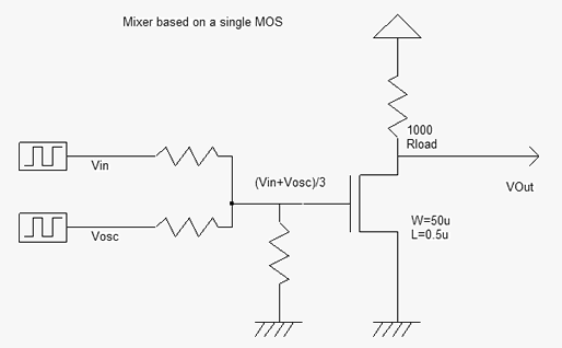 |
| Figure 12-75. Building a single-balanced mixer with a n-channel MOS device |
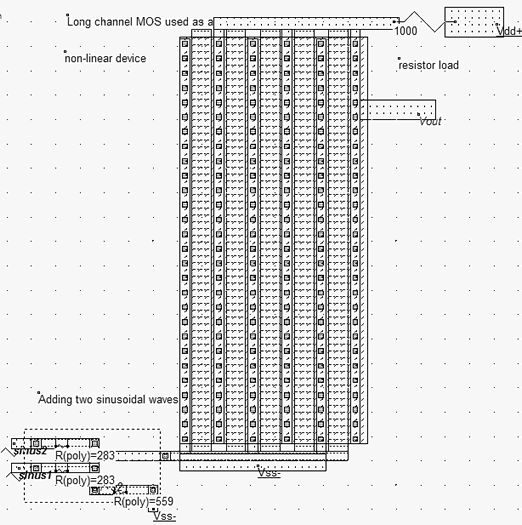 |
| Figure 12-76. Design of a mixer using a large width, large length nMOS device, with a sum of sinusoidal waves at the input |
Notice the unusually aspect of the MOS device in the layout shown in figure 12-76. Five gates are connected in parallel which are equivalent to one single MOS with the sum of channel width, but at the same time, the length is enlarged to obtain a sufficient quadratic dependence between voltage and currents, which is the main origin of harmonics . According to the theory, the time-domain simulation of the mixer reveals that the signal Vout has a very complex aspect (Figure 12-77).
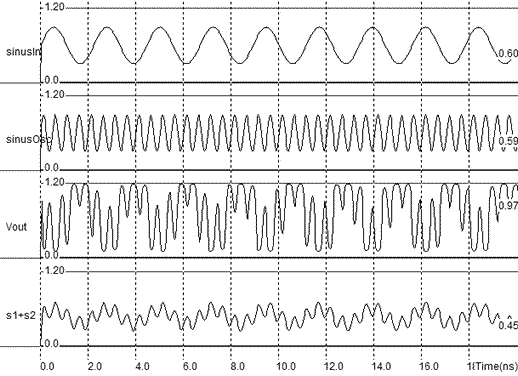 |
| Figure 12-77. Simulation of the mixer with a 450 MHz and "GHz added inputs |
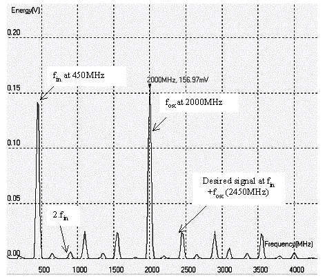
The Fourier Transform is obtained by a click on "FFT" in the simulation window (Figure 12-78). The 450MHz input signal, the 2GHz oscillator signal, as well as the harmonics and products are present in the spectrum. The only desired harmonic is the 2.45GHz contribution, corresponding to fin+fosc.
 |
| Figure 12-78. The output voltage includes fin, fosc and their corresponding harmonics. The desired signal is at fosc+fin |
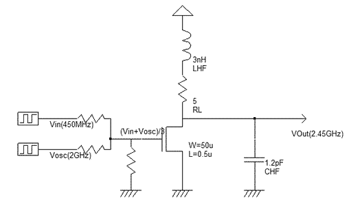
The mixer shown in figure 12-79 has two important features: the serial resistor is replaced by an inductor LHF of 3nH, and a capacitor CHF=1.2pF is added to the output. The LC resonator formed by the inductor LHF and the capacitor CHF matches the target frequency 2.45GHz (Use the resonant frequency evaluator in the Analysis menu to confirm). The serial resistor RL accounts for the finite quality of the inductor, and corresponds to the long metal wire resistance of the physical inductor. Removing this serial resistor would create overestimated oscillations, possibly numerical instability, and the results could not be exploited.
 |
| Figure 12-79. The schematic diagram of a mixer with a LC resonator tuned to 2.45GHz |
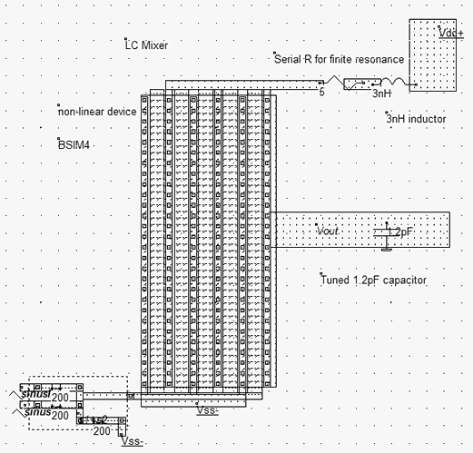
The mixer implementation has not been completed in the layout of figure 12-80. For simplicity, we used virtual L and C rather than a physical inductor. The 3nH inductor is placed in series with a parasitic resistance, which accounts for the physical serial resistance of the on-chip inductor, and limits the LC resonance effect. The capacitor 1.2pF is also virtual, and is placed near Vout.
 |
| Figure 12-80. The mixer with a tuned LC resonator targeted to 2.45GHz |
 |
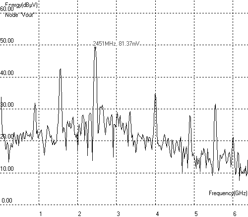
| Figure 12-81. The Fourier transform of Vout shows a main contribution at the desired frequency and residues of other harmonics |
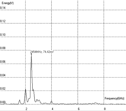
The Fourier transform of the time-domain simulation is proposed in figure 12-81, and corresponds to the output node Vout. The desired signal at 2.45GHz appears much more clearly than in figure 12-78, because of the pass-band passive resonator centered around that frequency. Unfortunately, the selectivity of the LC circuit is not high enough to erase the oscillator frequency at 2GHz. Residues of other harmonics also appear in the Fourier transform: 1.6GHz, 4GHz.
An increase of the input frequency fin is translated into a corresponding increase of the output frequency. For example, a slow increase in fin shifts the main peak to the right in a proportional way. Also, an increase of the amplitude of fin induces a corresponding increase of the 2.45GHz harmonic. This property is illustrated in figure 12-82 by adding a regular increase of the sinusoidal input (Parameter Increase f).
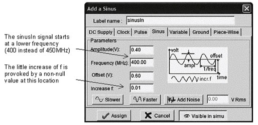 |
| Figure 12-82. The input SinusIn starts from 400MHz and slowly rises to 500MHz |
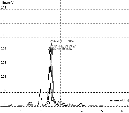 |
| Figure 12-83. A little increase of the input frequency is translated into an increase of the main harmonic |
The evolution of the FFT of Vout shows a shift in the peak resonance, due to the fact that the input sinusoidal wave has also shift toward high frequencies. This illustrates an important property of mixers that are conservative in terms of amplitude and frequency variations, except that the output frequency is situated at a fixed distance of the the input frequency.
The main drawback of the mixer output provided by the LC mixer is the important amount of parasitic signals added to the desired signal. The undesired signals 2.55GHz (fosc-fin), 2GHz (fosc), 2.9GHz (fosc+2.fin), 4GHz (2.fosc), appear in the spectrum and should be eliminated. A very brilliant idea would consist in creating two signals where all harmonics would be in opposite phase except the desired harmonics which would be in phase. Adding these two signals would create a miraculous signal with fosc+fin and fosc-fin.
 |
| Figure 12-84. Implementation of the double-balanced mixer |
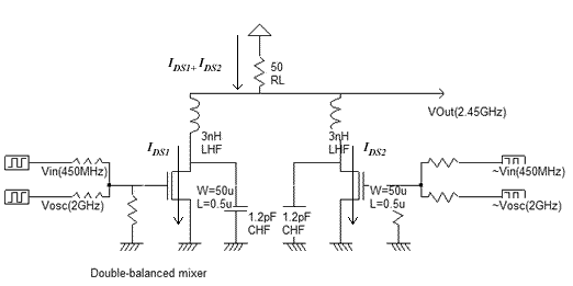
A circuit that realizes this function is proposed in figure 12-84. The signals vin and Vosc are combined as seen previously, in the left branch of the mixer, on the gate of the n-MOS device. The current that flows on the left nMOS device is Ids1, which can be approximated by equation 12-18. In the right branch of the mixer, the signals ~vin and ~vosc, representing the same signals as vin and vosc but with an opposite phase, are combined on the gate of the second n-MOS device. The current that flows on the right nMOS device is Ids2, which can be approximated by equation 12-19.
| (Equ. 12-18) | |
| (Equ. 12-19) |
Developing equation 12-18 and 12-19, the sum can be arranged as:
| (Equ. 12-20) |
The remarkable point that can be seen in equation 12-20 is that the sum of currents Ids1+Ids2 that flows in the 50ohm load resistor RL mainly includes a constant value Ids0 and the mixer products at frequencies fosc+fin and fosc-fin, which was exactly the goal of the mixer.
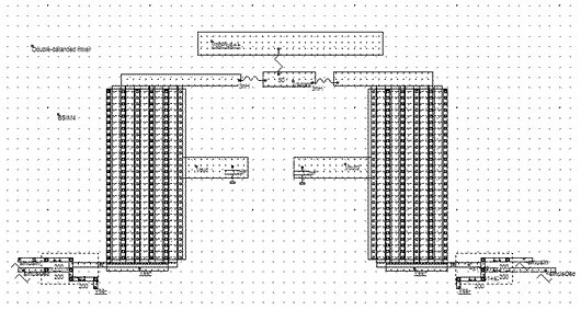 |
| Figure 12-85. Layout of the double-balanced mixer |
The layout implementation (Figure 12-85) makes an extensive use of virtual R,L,C elements. This technique is recommended for the tuning of the circuit, but one should remember that the final goal is a complete layout implementation. The simulation performed in figure 12-86 confirms the theoretical assumption: the Fourier transform clearly includes the two main contributions near 1500MHz and 2500Mhz, without fosc in between. Removing the undesired harmonics is quite easy, in order to keep the desired 2500MHz contribution.
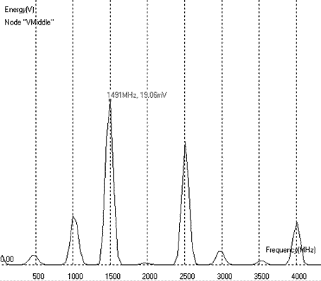 |
| Figure 12-86. Fourier transform of the double-balanced mixer output |
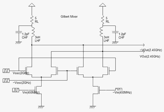 |
| Figure 12-87. The Gilbert mixer |
The double-balanced mixer is not implemented using a resistor based voltage adder, as suggested in the schematic diagram shown previously (Figure 12-84). Most mixers use the Gilbert cell [Gilbert], which consists of only six transistors, and performs a high quality multiplication of the sinusoidal waves [Lee]. The schematic diagram shown in figure 12-87 uses the tuned inductor as loads, so that Vout and ~Vout oscillate around the supply VDD.
 |
| Figure 12-88. The Gilbert mixer implementation with virtual R, L and C |
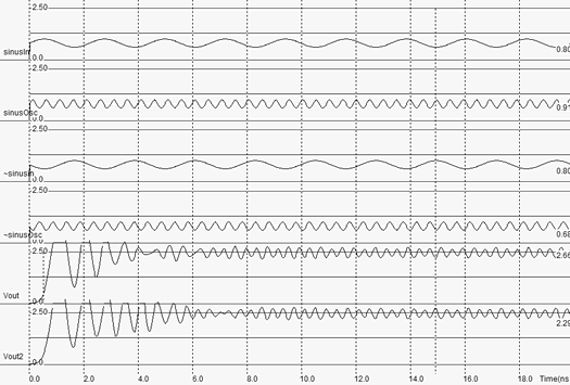 |
| Figure 12-89. Time-domain simulation of the Gilbert mixer |
The implementation shown in figure 12-88 makes again an extensive use of virtual R,L and C elements. The 3nH inductor is in series with a parasitic 5 ohm resistance, on both branches. The time domain simulation reveals a transient period from 0.0 to 8ns during which the inductor and capacitor warm-up. This initialization period is not of key interest. The most interesting part starts from 8ns, where the output Vout and Vout2 are stable, and oscillate in opposite phase around 2.5V.
 |
| Figure 12-90. Fourier transform of the Gilbert mixer output |
The Fourier transform of nodes Vout and Vout2 are almost identical. We present the Fourier transform in logarithm scale to reveal the small harmonic contributions. As expected, the 2GHz fosc signal and 450MHz fin signals have disappeared, thanks to the cancellation of contributions. The two major contributors fosc+fin and fosc-fin.
Notice that the simulation time has an influence on the Fourier Transform result: a short simulation (5ns) would a poor precision in our frequency range of interest, but a high precision on very high frequencies (Above 10GHz). In our case, it is preferable to perform the time domain simulation over a large time (50ns) which will give a high precision at low frequencies (From DC to 5GHz), but limit the Fourier spectrum to around 10GHz. As the target frequency is around 2.5GHz, a 50ns simulation gives the best results.
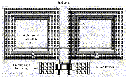 |
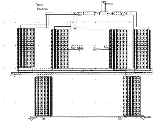
| Figure 12-91. The complete implementation of a Gilbert mixer circuit |
In figure 12-91, a complete implementation of the Gilbert mixer has been realized, so that virtual R,L and C components are replaced by physical elements. The coils have a target 3nH inductance, and their associated parasitic resistance is approaching 6 ohm when the combination of metal6,metal5 and metal4 are used. The tuning capacitor is added to the parasitic coil capacitor to perform the best resonance at the desired 2.5GHz frequency. The design relies on good models for the inductor and capacitor, which is not the case in the Microwind software, which uses first order approximations of parasitic resistance, capacitance and coil inductance. In a real case implementation, we may expect significant differences between measurements and simulations. Having accurate predictions of such circuits is quite challenging.
| Radio-Frequency Circuits > Frequency Converter |