| CMOS Design > MOS Modeling |
A family of models has been developed at the University of Berkeley for the accurate simulation of sub-micron technology. The Berkeley Short-channel IGFET Model (BSIM) exist in several version (BSIM1, BSIM2, BSIM3). The BSIM3v3 version promoted by the Electronic Industries Alliance (EIA) is an industry standard for deep-submicron device simulation.
A new MOS model, called BSIM4, has been introduced in 2000. A simplified version of this model is supported by Microwind2, and recommended for ultra-deep submicron technology simulation. BSIM4 still considers the operating regions described in MOS level 3 (linear for low Vds, saturated for high Vds, sub-threshold for Vgs<Vt), but provides a perfect continuity between these regions. BSIM4 introduces a new region where the impact ionization effect is dominant. In that region, Vds is very high, over the nominal supply voltage VDD. One of the key features of BSIM4 is the use of one singly equation to build the current, valid for all operating modes. Smoothing functions ensure a nice continuity between operating domains.
The number of parameters specified in the official release of BSIM4 is as high as 300. A significant portion of theses parameters is unused in our implementation. We concentrate on the most significant parameters, for educational purpose. The set of parameters is reduced to around 20.
| BSIM4 was created for analog submicron simulation 100 principal parameters |
|
| BSIM4 gives: |  |
|
|
| Many kinds of parameters | |
|
|
| A limitation procedure force parameters in their validity domain | |
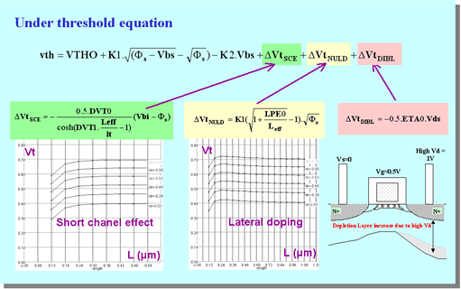
VTHO is the long channel threshold voltage at Vbs=0 (Around 0.5V), K1 is the first order body bias coefficient (0.5 V1/2), Φs is the surface potential, Vbs is the bulk-source voltage, K2 s thge second order body bias coefficient, &DeltaVtSCE is the short channel effect on Vt, ΔVtNULD is the non-uniform lateral doping effect explained in the equation, ΔVtDIBL is the drain-induced barrier lowering effect of short channel on Vt.
DVT0 is the first coefficient of short-channel effect on the threshold voltage (2.2 by default), DVT1 is the second coefficient of short-channel effect on the threshold voltage (0.53 by default), Leff is the effective channel length, and lt is the characteristic length, approximated in our implementation to 1/4 of the minimum channel length (0.03 µm for a 0.12µm ), Vbi is defined in the equation, and Φs is the surface potential.
The main impact of the Vt decrease is the Ioff parasitic current, detailed in the next paragraphs, that exhibits an exponential dependence with 1/Vt. Consequently, short channel MOS devices consume a very high standby current, which impacts the power consumption of the whole circuit.
The lateral drain diffusion (LDD) is a technique introduced in recent technologies to reduce the peak channel fields in the MOS channel.
For decreasing length, the threshold voltage tends to increase first (due to ΔVtNULD), before decreasing rapidly due to the short channel effect ΔVtSCE described.
When we apply a positive voltage on the drain of a long-channel n-MOS device, we observe no significant change in the value of Vt. When we do the same for a short-channel n-MOS device, we observe a decrease of the threshold voltage. The physical origin of DIBL is the increase of the depletion layer due to a high value of Vdrain, that reduces the equivalent channel length, and consequently decreases the threshold voltage.
| CMOS Design > MOS Modeling > BSIM4 |