| CMOS Design > MOS Modeling |
The five main capacitance considered in our implementation of MOS model 3 are:
The variation of the capacitance must be computed at each iteration of the analog simulation, for accurate prediction of the switching delay. The junction capacitance for drain and source have a significant contribution to the MOS capacitance.
| Parasitic capacitances play an important role: |
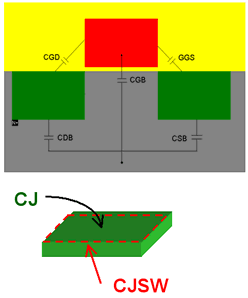
| CGD/CGS : grid/drain and grid/source -- depend on VGS and VDS -- fixed in model 1 -- well predicted by MM9, BSIM4 |
| CDB/CSB: drain/substrate and source/substrate -- composed by CJ and CJSW CJ: surfacic junction capacitance CJSW: peripheric junction capacitance périphérique de jonction |
| CGB or Cox : grid/substrate (gate oxyde capacitance) |
30
parameters in BSIM4 for capacitance model ! |
| CMOS Design > MOS Modeling > Dynamic Behavior |