| Radio-Frequency Circuits > Inductor |
Inductors are commonly used for filtering, amplifying, or for creating resonant circuits used in radio-frequency applications. On-chip inductance have typical values ranging from 1 to 100nH, which give an equivalent impedance between 10 and 1000 ohm, within the radio-frequency range 300MHz-3GHz (Figure 12-2). At frequencies lower than 100Hz, discrete off-chip as used because of the high inductor values (From 1to 100µH) to keep the impedance between 10 and 1000 Ohm. Such high inductances cannot be integrated in a reasonable silicon area. Around 1GHz, a 10nH on-chip inductor matches the standard 50Ω impedance of most input and output stages in very high frequency applications.
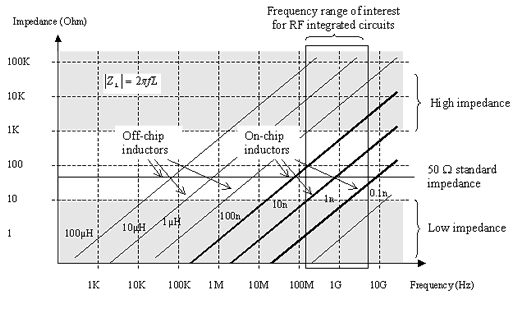 |
| Figure 12-2. The inductor impedance versus frequency |
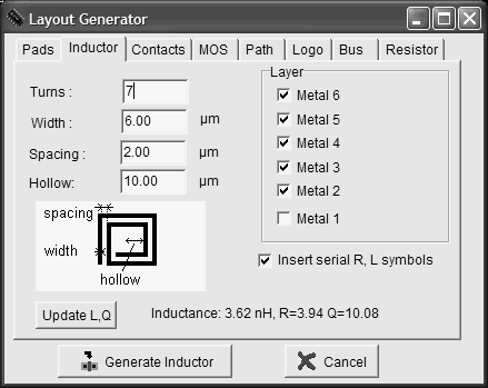
The layout of a 10nH inductor is typically a square spiral, since standard CMOS processes constrain all angles to be 90° (Figure 12-3). When possible, a polygon spiral using 45° tracks is used to increase the electrical performances of the inductor. We investigate here the design of a rectangular on-chip inductor, the layout options and the consequences on the inductor quality factor. The inductor can be generated automatically by Microwind using the command Edit > Generate > Inductor . The menu is reported in figure 12-3. The inductance value appears on the bottom of the window, as well as the parasitic resistance and the resulting quality factor Q.
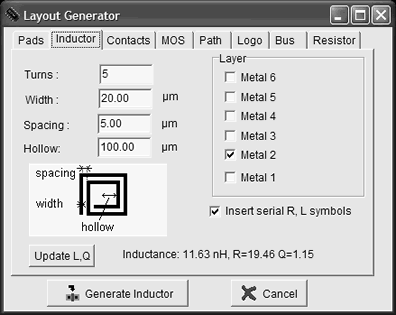 |
| Figure 12-3. The inductor generator menu |
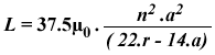
There exist a huge number of inductance calculation techniques, as detailed in the review from [Thompson]. A very interesting discussion about square planar spiral inductor may be found in [Lee]. The inductance formula used in Microwind (Equation 12-1) is one of the most widely known approximation, proposed as early as 1928 by [Wheeler], which is said to be still accurate for the evaluation of the on-chip inductor. With 5 turns, a conductor width of 20µm, a spacing of 5µm and a hollow of 100µm, we get L=11.6nH.
 |
(Equ. 12-1) |
| with r = n.(w + s) µ0=4π.10-7 n=number of turns w= conductor width (m) s=conductor spacing (m) r=radius of the the coil (m) a=square spiral’s mean radius (m) | |
The quality factor Q is a very important metric to quantify the resonance effect. A high quality factor Q means low parasitic effects compared to the inductance. The formulation of the quality factor is not as easy as it could appear. An extensive discussion about the formulation of Q depending on the coil model is given in [Lee]. We consider the coil as a serial inductor L1, a parasitic serial resistor R1, and two parasitic capacitor C1 and C2 to the ground, as shown in figure 12-4. Consequently, the Q factor is approximately given by equation 12-2.
 |
(Equ. 12-2) |
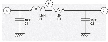 |
| Figure 12-4. The equivalent model of the 12nH default coil and the approximation of the quality factor Q |
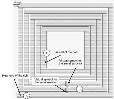
Using the default parameters, the coil inductance approaches 12nH, with a quality factor of 1.15. The corresponding layout is shown in figure 12-5. Notice the virtual inductance (L1) and resistance (R1) symbols placed in the layout. These symbols indicate to the extraction that that three separate electrical nodes are requested (A,B and C), with a serial inductor between A and B and a serial resistance between B and C. If these symbols were omitted, the whole inductor would be considered as a single electrical node. Only the capacitance (C1, C2) would be properly extracted.
 |
| Figure 12-5. The inductor generated by default |
A high quality factor Q is attractive because it permits high voltage gain, and high selectivity in frequency domain. The usual value for Q is between 3 and 30. The main limiting factors for Q are the serial resistance R1 of the wire and the substrate coupling capacitor C1 and C2. From equation 12-2, it clearly appears that R1,C1 and C2 should be kept as low as possible to increased Q. There are several ways to improve the coil quality factor. The first one consists in using the upper metal layer (metal 6 in 0.12µm), which features a smaller sheet resistance together with a smaller capacitance. Unfortunately, the quality factor is only increased to 2.
A significant improvement consists in using metal layers in parallel (Figure 12-6). The selection of metal2, metal3, up to metal6 reduces the parasitic resistance of R1 by a significant factor, while the capacitance of C1 and C2 is not changed significantly. The result is a quality factor near 6. Even when the conductor width is increased to further reduce R1, or if the number of turns and the coil shape is changed, the maximum Q is almost invariably below 10.
 |
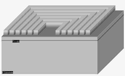 |
| Figure 12-6. A 3D view of a high Q inductor using metal layers in parallel |
The coil can be considered as a RLC resonant circuit. A very low frequencies, the inductor is a short circuit, and the capacitor open circuits (Figure 12-7 left). This means that the voltage at node C is equal to A if no load is connected to node C. At very high frequencies, the inductor is an open circuit, the capacitor a short circuit (Figure 12-7 right). Consequently, the link between C and A tends to an open circuit.
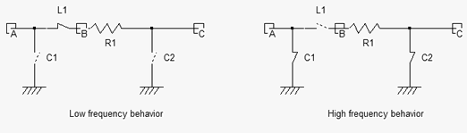 |
| Figure 12-7. The behavior of a RLC circuit at low and high frequencies |
At a very specific frequency the LC circuit features a resonance effect. The theoretical formulation of this frequency is given by equation 12-3.
 |
(Equ. 12-3) |
 |
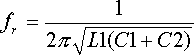
| Figure 12-8. The resonance frequency depending on the capacitance and inductance |
The variation of the resonant frequency with the capacitor and inductor is proposed in figure 12-8. On-chip coil inductance are within the range of 1 to 100nH. As the capacitance may vary from 1pF to 1nF, the range of the resonant frequency is around 100MHz to 10GHz, which includes most of the radio-frequency designs.
 |
| Figure 12-9. Microwind can computes the resonance frequency corresponding to user-defined L and C values |
In the Analysis menu, the command Resonance Frequency includes a resonant frequency calculator, as shown in figure 12-9. For a given value of inductor and capacitor (3nH and 1.4pF in this example), the resonant frequency is computed, directly in mega-hertz (MHz). For a target frequency of 2.45GHz, and a given inductor value of 3nH, we must choose a capacitor close to 1.4pF.
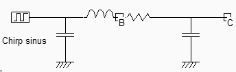
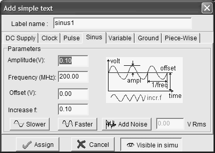
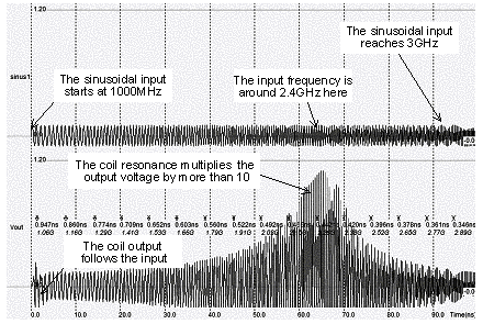
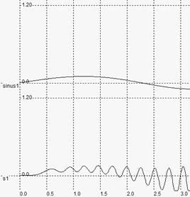
In the case of L1=3nH (Design corresponding to figure 12-6), the total capacitor is around 7pF. From the abacus given in figure 12-8, we obtain a resonant frequency around 1GHz. We may see the resonance effect of the coil and an illustration of the quality factor using the following procedure. The node A is controlled by a sinusoidal waveform with increased frequency (Also called "chirp" signal). We specify a very small amplitude (0.1V), and a zero offset. The resonance can be observed when the voltage at nodes B and C is higher than the input voltage A. The ratio between B and A is equal to the quality factor Q.
 |
 |
| Figure 12-10. Using a sinusoidal waveform with increased freauency |
 |
| Figure 12-11. The behavior of a RLC circuit near resonance |
The frequency corresponding to the resonance is around 2.4GHz, as predicted by the theoretical formulation. However, some mismatch between the prediction and the simulation may appear: first of all, the sinusoidal generator forces node A to a given voltage, which inhibits the role of capacitor C1. The resonance is only based on L1, R1 and C2, which shifts the frequency to higher frequencies. Secondly, the simulation of the inductor effect requires a significant amount of computation, with a high precision, otherwise the simulation becomes unstable. In 0.12µm, the simulation step is fixed to 0.3ps, which is a good compromise between accuracy and speed. However, when dealing with inductor, this step should be reduced. IF we increase the step to 1ps (Figure 12-12-a), an important parasitic instability effect appears and the output tends to oscillate. With a small simulation step (0.1pS in the case of figure 12-12-b), the simulation converges but the computation is significantly slowed down.
 |
 |
| (a) Simulation step 1ps - too large | (b) Simulation step 0.1ps - correct |
| Figure 12-12. The numerical instability appears in the inductor simulation when using a large integration interval (1ps), which is removed when lowering this interval to 0.1ps. | |
| Radio-Frequency Circuits > Inductor |