| Radio-Frequency Circuits > Power Amplifier |
The power amplifier is part of the radio-frequency transmitter, and is used to amplify the signal being transmitted to an antenna so that it can be received at the desired distance. A numerical or analog information is processed at low frequency, and converted to an appropriate sinusoidal waveform combined with a modulation. The high frequency converter transforms the low frequency signal flow to a high frequency signal fhigh. The shape of fhigh is identical to flow except that the frequency is one or two orders of magnitude higher. Details about this circuit are provided later in this chapter. The amplitude of fhigh is usually small (10-100mV). A power amplifier is required to multiply the amplitude of the signal in order to transmit enough power to the emitting antenna.
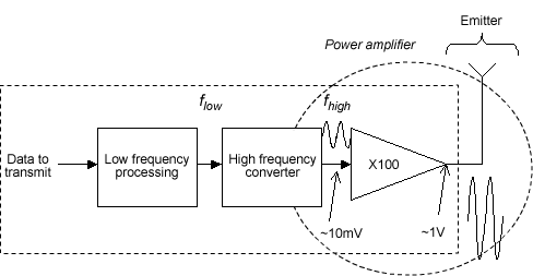 |
| Figure 12-13. The power amplifier in a typical radio-frequency system |
We can consider an antenna as a load that, in the ideal case, will be a pure resistance. The antenna resistance Ra accounts for the power absorbed by the antenna and appearing at the termination point of the power amplifier. This power is mainly radiated by the antenna. Most mobile phone antennas are resonant monopole [Macnamara] for which the antenna resistance Ra varies from 20 Ω (Ground plane width w=0) to 40 Ω (Infinite ground plane width). The monopole radiates mainly on X and Y directions (Figure 12-14). The length of the antenna is often chosen close from λ/4, where λ is the wavelength of the emitted signal. That length corresponds to a maximum in the sinusoidal wave. From an electrical point of view, we can modelize the antenna as a pure resistive load. The value of 50ohm is commonly used for Ra in simulations, as most equipments are "50 ohm adapted".
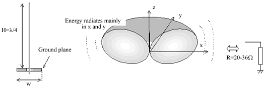 |
| Figure 12-14. In first approximation, the antenna can be approximated as a lload resistance around 30 Ω |
The level of output power in mobile phones ranges approximately from 10mW to 1 Watt. The usual unit for qualifying the power is the dBm, meaning "dB milliwatt". The correspondence between the Watts and the dBm is given below. A 1Watt amplifier has an output power Pout of 30dBm (Equation 12-4).
 |
(Equ. 12-4) |
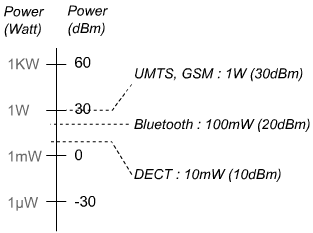 |
| Figure 12-15. Correspondence between watts and dBm for several radio frequency systems |
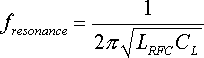
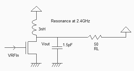
Most CMOS power amplifiers are based on a single MOS device, loaded with a "Radio-Frequency Choke" inductor LRFC, as shown in figure 12-16. The power is delivered to the load RL, which is often fixed to 50Ohm. This load is for example the antenna monopole, which can be assimilated to a radiation resistance, as described in the previous section. The resonance effect is obtained between LRFC and CL. The formulation for resonance is given below.
 |
(Equ. 12-5) |
 |
| Figure 12-16. The basic diagram of a power amplifier |
For example, a power amplifier designed for Bluetooth operation should resonate around 2.4GHz. If we assume that the inductance has a value of 3nH, the corresponding capacitor is around 1.5pF.
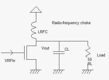
The MOS devices used in power amplifier designs have very huge current capabilities, to be able to deliver strong power on the load. This leads to very unusual constraints to the width of the transistor: devices with a width larger than 1000µm are commonly implemented [Hella]. The radio frequency choke inductor has a resonant effect which induces and important voltage swing of node Vout. Consequently, high voltage MOS devices are used to handle large overvoltage. A MOS device with a very large width is not drawn directly, but is obtained by connecting medium size MOS devices in parallel. In Microwind, we generate easily multiple-finger MOS devices, thanks to the MOS generator command (Figure 12-17). The high voltage option is selected, and the number of fingers is fixed to 10.
 |
| Figure 12-17. Generating a transistor with large current capabilities |
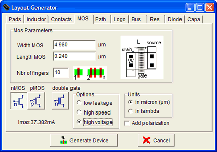
The layout generated by Microwind is completed by adding a polarization ring to VSS, and metal2 contacts to the gate (Signal VRF_In) and the drain (Signal Vout). The result is shown in figure 12-18. The maximum current is close to 40mA. A convenient way to generate the polarization ring consists in using the Path generator command, and selection the option Metal and p-diffusion. Then draw the location for the polarization contacts in order to complete the ring.
 |
| Figure 12-18. The layout of the power MOS also includes a polarization ring, and the contacts to metal2 connections to VRF_in and Vout |
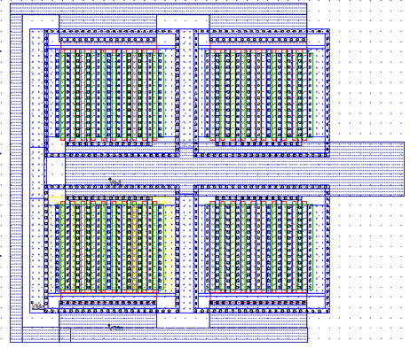 |
| Figure 12-19. The layout of a 160mA power MOS using four large MOS in parallel |
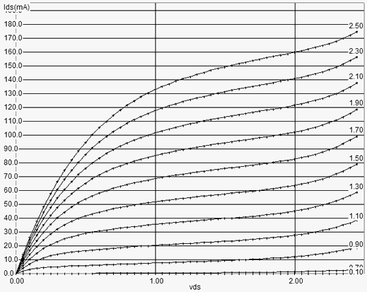 |
| Figure 12-20. The static charasteristics of the 160mA power MOS |
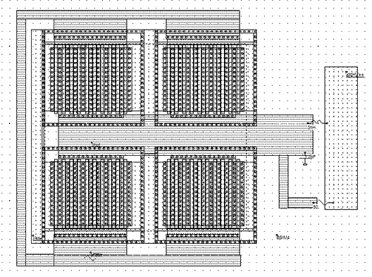
An example of 160mA power device is shown in figure 12-19. Four devices are connected in parallel. The output node drives a large current and must be designed as wide as possible, with a short connection to the output pad, to limit the serial resistance and parasitic capacitor to ground. The ESD protection is removed in some cases, to enhance the power amplifier performances [Hella]. In the characteristics Id/Vd, the maximum Ion current is close to 170mA (Figure 12-20). The ground connection also drives a strong current and must be carefully connected to the ground supply.
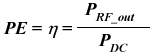
One of the most important characteristic of the power amplifier is the power efficiency, also called "drain efficiency" [Lee]. The definition of drain efficiency is given by equation 12-6. The power efficiency is a ratio between the power delivered to the load and the supply power. The power efficiency (PE) is usually given in %. Typical PE range from 25 to 50%.
 |
(Equ. 12-6) |
| Where PRF_out is the RF output power (in watt) PDC is the total power delivered from the supply (in watt) | |
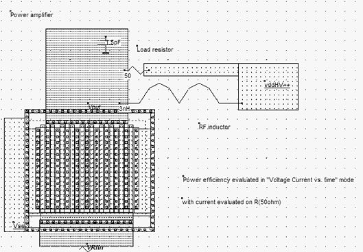
We may evaluate the power efficiency of the power amplifier with Microwind, using the following simulation procedure. The power amplifier is designed with a virtual load (RL=50 ohm in the case of figure 12-21). Notice that the connection of the RL virtual load is unusual: one end of the resistor is connected to VDD rather than VSS.
Connecting RL to ground would add a very important standby DC current, flowing through RL even without RF input. In reality, the RL resistor represents the antenna radiation resistance which has no direct path to ground. To avoid the parasitic DC contribution, we connect one end of RL to VDD.
 |
| Figure 12-21. The evaluation of the power amplifier efficiency |
The layout corresponding to the power amplifier is shown in figure 12-22. The inductor is virtual, as well as the 50ohm load. By default, the power PDC is computed at each simulation and appears at the right lower corner of the simulation window of Microwind. In the simulation window corresponding to the mode Current And Voltage vs. time, we select the current flowing in R(50ohm). At the end of the simulation (Figure 12-23), the evaluation of the power efficiency is also displayed.
 |
| Figure 12-22. The evaluation of the power amplifier efficiency |
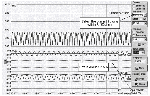 |
| Figure 12-23. The evaluation of the power amplifier efficiency is accessible in the "Voltage and Current vs. Time" mode, by selecting the virtual load |
From the simulation of the simple power amplifier, we obtain a power efficiency of 2.5%, which is extremely low (Figure 12-23). In other words, 97.5% of the supply energy is dissipated and lost in the circuit, with only 2.5% delivered to the load. There are several techniques to improve the power efficiency: increase the MOS size, modify the amplitude of the input sinusoidal wave, and modify the DC offset of the input sinusoidal wave.
An other metric for the power amplifier efficiency is the power added efficiency or PAE [Hella]. The PAE is very similar to equation 12-6. It includes the input power PRF_in as given in equation 12-7. Microwind do not evaluate directly this parameter.
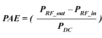 |
(Equ. 12-7) |
| Where PRF_out is the RF output power (in watt) PRF_in is the RF input power (in watt) PDC is the total power delivered from the supply (in watt) | |
The distinction between class A,B,AB, etc.. amplifiers is mainly given with the polarization of the input signal. A Class A amplifier is polarized in such a way that the transistor is always conducting. The MOS device operates almost linearly. An example of power amplifier polarized in class A is shown in figure 12-24. The power MOS is designed very big to improve the power efficiency.
 |
| Figure 12-24. The class A amplifier design with a very large MOS device |
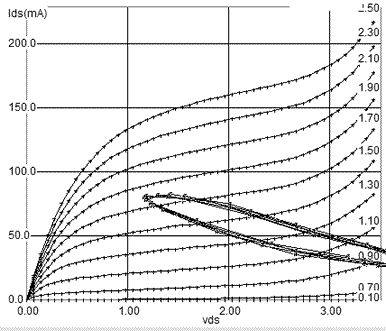
The sinusoidal input offset is 1.3V, the amplitude is 0.4V. The power MOS functional point trajectory is plotted in figure 12-25, obtained using the command Simulate on Layout. We see the evolution of the functional point with the voltage parameters: as Vgs varies from 0.9V to 1.7V, Ids fluctuates between 20mA to 70mA. The MOS device is always conducting, which corresponds to class A amplifiers.
 |
| Figure 12-25. The class A amplifier has a sinusoidal input |
The main drawback of Class A amplifiers is the high bias current, leading to a poor efficiency. In other words, most of the power delivered by the supply is dissipated inefficiently. The power efficiency is around 11% in this layout. The main advantage is the amplifier linearity, which is illustrated by a quasi-sinusoidal output Vout, as seen in figure 12-26.
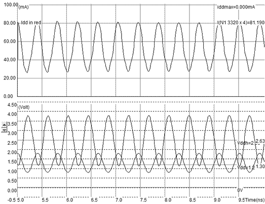 |
| Figure 12-26. The class A Amplifier simulation |
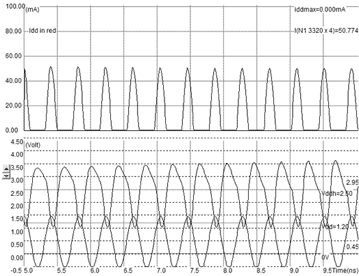
In class B, the MOS device only conducts for half a cycle. The monitoring of the current flowing in the power MOS shows a peak of current during half the input period. During the other half, the power MOS is off, and the LC resonator transmits the power to the 50 ohm load. The power efficiency rises to 20%. The main drawback is the severe distortion of the output voltage, which was much less visible on the class A polarization. The intermediate class, called AB, corresponds to a conduction between half and the full cycle.
 |
| Figure 12-27. The class distinction for the power amplifier is linked to the DC value of the input signal |
An evaluation of the spectral contents of the output node may be performed by the Fourier transform, with a plot in logarithmic scale. The Fourier transform is accessible on the simulation menu, through the button FFT. The fast Fourier transform translates the voltage waveform of the selected node into an evaluation of the energy of the signal versus the frequency. The plot of the energy shown in figure 12-28 reveals a peak near 2.5GHz. A noticeable energy is found on the second harmonic (2.f0=4900MHz) and third harmonics (3.f0). This is the consequence of a non-linear amplifier device.
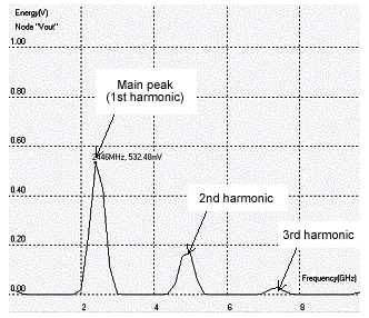 |
| Figure 12-28. The class B amplifier is less linear than class A amplifier |
In class C, the conduction occurs during less than half the cycle. The increase of efficiency obtained by reducing the conduction period is achieved at the expense of a reduced output power delivered to the load. The class E amplifier schematic diagram is shown in figure 12-29. A band pass filter (LHF, CHF) is added to the output stage, fitted to the VRFin input frequency. The effect of this passive circuit is to decrease the amplitude of the parasitic harmonics due to the non-linear nature of the amplifier, and to pass the desired frequency contribution. In some particular cases, the 3rd or even 5th harmonic is the desired one (Such as is 77GHz automotive radars for example, where the amplifier also serves as a frequency shifter).
The power stage is coupled to the resonator through a coupling capacitor Cc. The role of Cc is to transfer the energy to the load, without any DC path between the supply and the load. The MOS drain can reach very high values when the switch is OFF. Consequently, a high breakdown voltage transistor is required. The theoretical efficiency of class E amplifier is higher than 50%.
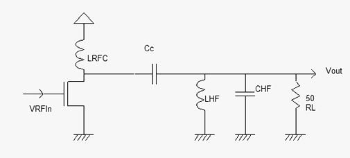 |
| Figure 12-29. Class E amplifier |
Self heating refers to the temperature rise that can occur in power devices, due to excessive heat energy accumulated before being dissipated through the substrate, the package and ultimately through the air. The thermal time constant is the order of one micro-second. Simulations usually consider a typical temperature of 25°C. This is realistic in the case of low power dissipation (Some milli-watts). In the case of hundreds of milliwatts, the simulation show take in account a significant temperature rise near the device. For example, a temperature of 80°C is commonly considered in medium power devices (Below 1W). In some cases, the IC may operate up to 250°C. In Microwind, the operating temperature may be changed in the menu Simulator Parameters of the simulation menu. In the window shown in figure 12-30, the temperature is fixed to 85°C.
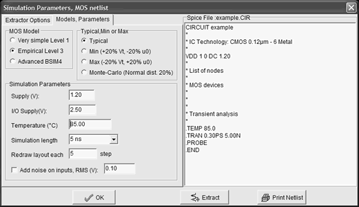 |
| Figure 12-30. Setting up a high temperature for analog simulation |
| Radio-Frequency Circuits > Power Amplifier |